
PROBoter - A platform for automated PCB analysis
Part I of the PROBoter blog post series
November 24, 2020
This is the first article of a four part blog post series that introduces this platform. The following topics will be discussed in this series:
- PROBoterdemovideo
- PartI:AplatformforautomatedPCBanalysis
- PartII:ThePROBoterhardwareplatform
- PartIII:VisualPCBanalysiswithNeuralNetworksandclassicComputerVisionalgorithms
- PartIV:Automatedvoltagesignalanalysisandprotocolidentification
- PartV:ThePROBotersoftwareframework
Securityanalysisofembeddedsystems on the Printed Circuit Board (PCB) level can be a very tedious and time-consuming task. Many steps like visual PCB inspection and reverse engineering of security relevant nets, i.e. electrically connected components, is usually done manually by an embedded security expert. Things get even worse when multiple hardware revisions of the same PCB must be examined. To support analysts in this field, the aim of the master’s thesis AutomatisierungderhardwarenahenSicherheitsanalysevoneingebettetenSystemen written at SCHUTZWERK in cooperation with HochschuleKempten was to find new ways to automate as many of the tasks required when doing PCB security analysis as possible. The result is a hardware and software platform called the PROBoter. The PROBoter’s main features are:
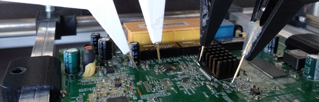
- A hardware platform that provides automated probing with up to four independent probes.
- A camera system that is fully integrated in the hardware platform to generate high resolution PCB images.
- Simple construction of the hardware platform based on standard parts and 3D printed components which facilitates easy and cost-efficient replication.
- Automated calibration of the whole platform to compensate linear errors related to manufacturing and the assembly process.
- Automated visual PCB analysis based on Neural Networks to localize Integrated Circuits (ICs) and their corresponding pins on PCB images.
- A click-and-probe software solution that utilizes the hardware platform for automated PCB image generation, visual analysis and (semi-)automated probing.
- The hardware design and software is open-source. Check out the PROBoterGithubrepository [1].
In this first part of the PROBoter blog post series the main idea behind the platform and basic concepts of embedded system security analysis are presented.
The manual process
When doing a security analysis of an embedded system, a few tasks must always be performed regardless of the system or device under test: First, the device’s PCB(s) must be uncovered by removing the surrounding enclosure. Sometimes it is even necessary to further disassemble the device by removing parts like heat sinks or coolers. After that, each PCB is scanned for components which are relevant to the system’s security. The analyst’s main focus is on active components. This includes data storage components like persistent memory chips that could contain sensitive data or intellectual property. Also, components that expose an interface to interact with the system, like microcontrollers or processors, are of interest. An attacker could abuse improperly configured interfaces to trick the system into performing unintended actions or revealing internal secrets.
Depending on the component package, i.e. the housing and pin layout, some pins of a component may not be directly accessible. One possible solution to still interact with them is to partially reverse engineer the electrical nets these components are connected to by following traces on the PCB. For example, security-relevant pins like the ones belonging to a debugging interface are often exposed either via pin connectors or test pads to allow for initial programming by the board manufacturer or to perform initial functional tests at the end of the production line.
After analyzing the PCB, a security analyst will try to interact with the system under examination. This is done by connecting chip programmers, memory readers or other analysis tools like the BusPirate [2] to the PCB or a single component. Depending on the PCB’s components, multiple attack vectors are possible and can now be examined by the analyst. Tests range from interacting with an exposed serial connection to dumping memory contents for offline analysis.
Sometimes the functionality of component pins is unknown to the analyst due to a lack of publicly available documentation. In this case, it is up to the analyst to reconstruct the missing information. For example, one method to identify pin functionalities is to analyze their signals at runtime. Communication buses often can easily be identified by comparing the recorded signals to well-known patterns.
The last step of each security analysis is to create a report for the customer. This document should describe all the identified system vulnerabilities in a clear and easy to understand way.
Let’s automate it
The main idea behind the PROBoter platform is to assist a security analyst in all tasks mentioned above. Most of these tasks should be performed by the PROBoter without any user interaction, therefore allowing the analyst to focus on the most important task, the security testing process itself. The first step while developing such an automation tool was to design an automated workflow of the embedded system security analysis based on the described manual process. The result is shown in the figure below.
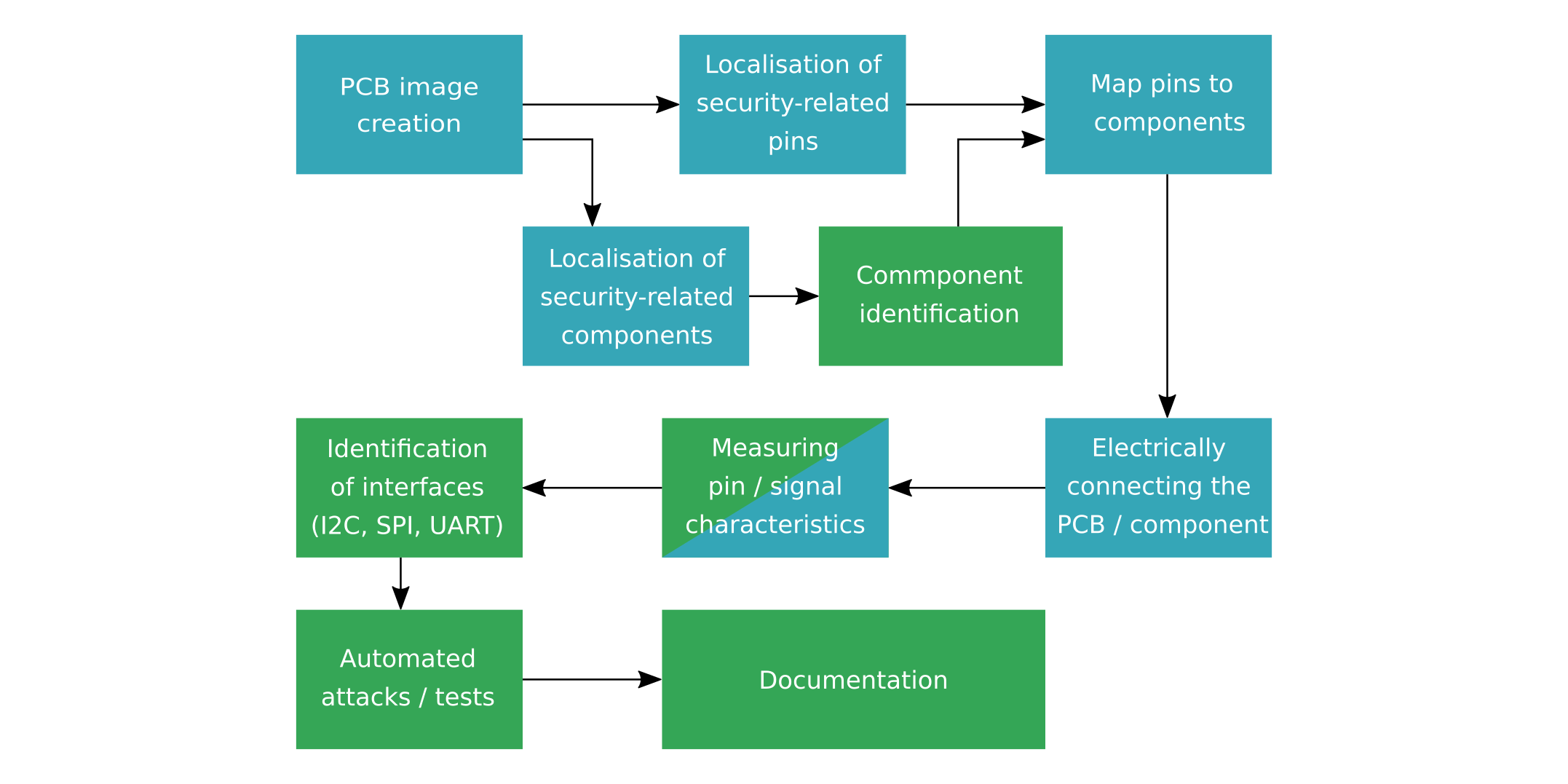
A generated high-resolution image of the PCB under test forms the base for all further automated analysis steps. During the first analysis step, the image data is processed to locate components that might be relevant for a security analyst, such as microcontrollers or memory chips. As this is basically an object detection task, methods based on state of the art Neural Network object detectors or classic Computer Vision algorithms could be utilized here. For each component found, an identification step should be performed to get information about the component’s functionality and possible external interfaces. The chip marking and package can be used during this step as key features to classify and identify a component.
To allow automated probing, the precise location of component pins and other possible probing locations like test pads have to be searched in the provided image data. This step can be performed simultaneously to the component localization and identification to reduce analysis time. If performed in parallel, a mapping between the identified pins and the located components is necessary. It is also possible during this step to map component functionality like debugging interface pins or data bus lines to identified pins. The required pinout could for example be extracted from datasheets provided by component manufacturers in an automated way.
All the analysis described so far is only based on image data of the PCB’s top and bottom side. For complex multi-layer PCBs, it is possible that important information like component interconnections may be hidden in the inner layers and can therefore not be detected by visual inspection. To fill this information gap, automated electrical probing in combination with electrical resistance measurements can be used to reconstruct pin or component connections not visible from the outside.
By measuring electrical signal characteristics during runtime in the next step, it is possible to identify communication buses in an automated way. This is especially useful if the chip identification step in the early analysis stage failed. There already exist some tools to identify common interfaces like JTAG. One popular tool that falls into this category is the JTAGulator [3] developed by Joe Grand. This tool can identify JTAG debugging interfaces automatically within a range of up to 24 pins connected to the device. During a scan, the JTAGulator sends defined JTAG commands to a permutated subset of the connected pins and listening on the other pins for a valid response. The tool can also assist in (semi-)automated UART pin identification.
With all the collected information about the PCB under test, automated security tests can then be performed. Applicable tests depend highly on the type of components that are used on a PCB. For example, an exposed serial interface might provide a login shell which allows for direct interaction with the operating system running on the embedded system. Data on communication interfaces like SPI or I2C can be passively sniffed or actively manipulated on-the-fly in a Man-in-the-Middle (MitM) setup. Debug interfaces can be checked for protection mechanisms or other security measures to name just a few.
Finally, the results of all performed analysis steps can be automatically documented and stored in a project-specific or central repository. When writing the final report, an analyst therefore has to consult only a single data source to access all relevant information. A single data repository also allows for easy collaboration as test results can be accessed simultaneously by many analysts. Analysis results can also be easily shared between projects. This enables building a common knowledge base which can reduce analysis time in future projects.
All the tasks shown in Figure 1 marked with a blue color can be done in a (semi-)automated way with the current version of the PROBoter platform. The framework focuses on tasks that require automated electrical probing and visual PCB analysis as these are the most repetitive and time-consuming ones. The analysis steps highlighted in green are currently not implemented but could be integrated in the framework in the future.
Next Post
After the introduction of the idea behind the project, the next post of this series, called ThePROBoterhardwareplatform
, will
focus on the heart of the PROBoter, a hardware platform for automated electrical
probing and PCB image generation. The PROBoter features an auto-calibration routine which will
also be described in detail.
Follow us on Twitter
, LinkedIn
, Xing
to stay up-to-date.
References / Credits
[1] https://github.com/schutzwerk/PROBoter
[2] http://dangerousprototypes.com/docs/Bus_Pirate
[3] http://www.grandideastudio.com/jtagulator/
[5] PROBoter paper https://doi.org/10.13154/294-8348
This work was sponsored by the BMBF project SecForCARs
.
We also want to thank igusGmbH
for their support and providing hardware samples.
The project was created at SCHUTZWERKGmbH
(supervisors Dr. Bastian Könings & Msc. Heiko Ehret) in cooperation
with HochschuleKempten
(examiners Prof. Dr. Elmar Böhler & Prof. Dr. rer. nat Stefan Frenz).