
Visual PCB analysis with Neural Networks and classic Computer Vision algorithms
Part III of the PROBoter blog post series
August 8, 2022
The list below gives an overview of the topics covered in this blog post series. Links will be updated as soon as the corresponding parts are being released.
- PROBoterdemovideo
- PartI:AplatformforautomatedPCBanalysis
- PartII:ThePROBoterhardwareplatform
- PartIII:VisualPCBanalysiswithNeuralNetworksandclassicComputerVisionalgorithms
- PartIV:Automatedvoltagesignalanalysisandprotocolidentification
- PartV:ThePROBotersoftwareframework
The lastpart of the PROBoter series introduced the heart of the PROBoter framework - the hardware platform. The platform allows (semi) automated electrical probing of an unknown PCB which is usually a very time consuming and error prone task. This post focuses on methods to automate the initial analysis step of an embedded system - the visual analysis of the PCB(s) forming the device under test.
An embedded pentester’s helping eye
If you start a penetrationtestofanembeddedsystem , the first step is usually to open the device under test to reveal the printed circuit boards (PCBs). These PCBs contain all the electrical and electronic components required for the device’s functionality. From a security perspective, we usually focus on components that either process information, like microcontrollers, or store data, like external flash memory chips. So we start with the localization of components that might be security-relevant and verify our assumption in the next step by identifying the component and its functionality based on the printed marking usually found on its plastic cover.
For each successfully identified component, we try to fetch additional information from technical data sheets or developer documentation usually found on the manufacturer’s website. The main goal here is to find information about the mapping of security-critical functionality, like debug or communication interface lines, to respective pins connecting the component to the underlying PCB. With this information, we finally connect to the component over the identified pins and can start communicating with it or extracting data.
If we take a step back, we can see that the visual analysis of a populated PCB is basically an object detection task where the instances to localize and identify are electronic components, electrical pins and contact pads. Object detection is an active research topic where great progress has been made in the last years with the introduction of Neural Networks and especially the subclass of Convolutional Neural Networks. So in order to assist an analyst during the visual analysis, the PROBoter platform contains algorithms based on Neural Networks and Classic Computer Vision to automatically localize integrated circuits (ICs) and their respective pins in image data of populated PCBs.
PCB and pin image data sets
To train a Neural Network or evaluate a Classic Computer Vision algorithm, you need some reference. Such data is usually provided in the form of annotated image data sets. For the task of PCB image analysis, there already exist some publicly available PCB image data sets, like the PCB-DSLRimagedataset [1] introduced by Pramerdorfer and Kampel. In addition, several data sets have been published in the last years. A selection can be found in our PROBoterpaper published at escar Europe 2021.
Most of these data sets are designed by their authors for a specific use case which is typically not the security analysis of an embedded system. Therefore, we introduce the following three new PCB image data sets that are also published in the PROBoterGithubrepo .
PCB-GOOGLE
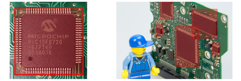
The first image data set PCB-GOOGLE is a collection of images collected using Google image search. It contains 190 images of populated PCBs and 1,100 manually labeled IC object instances. The images in this set show a wide variety of PCBs regarding solder mask color as their component package types and zoom levels ranging from macro views of single ICs to arrangements of multiple PCBs.
PCB-INTERNAL
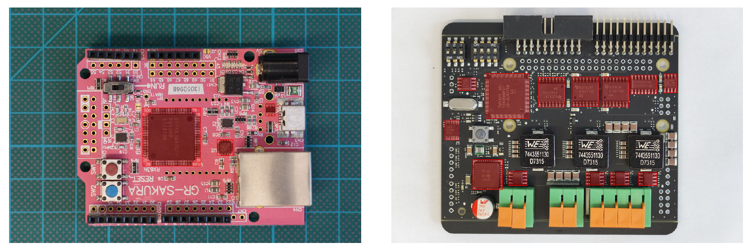
The second image data set is named PCB-INTERNAL. It is comprised of 15 unique PCB images with 53 annotated IC instances. The images contain publicly available development boards and PCBs designed by SCHUTZWERK employees.
IC-PINS
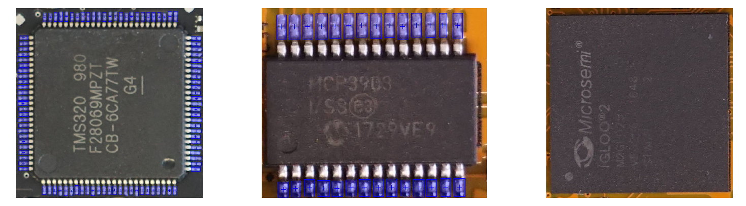
PCB-GOOGLE and PCB-INTERNAL are designed to train and test algorithms for IC localization. In contrast to these, our last image data set IC-PINS is specifically crafted for the use case of component pin detection. It contains 46 IC macro images with 1,181 annotated component pins. The number of pins per image ranges from zero visible pins for Ball Grid Array (BGA) packaged ICs up to 100 pins, typically found at Thin Quad Flat Packages (TQFP).
Component / IC detection
Based on these new PCB image data sets, we trained well-proven object detectors to localize ICs in image data of populated PCBs. We use the TensorFlowObjectDetectionAPI [2] as a base framework. Regarding the Neuronal Network architecture, we picked enhanced versions of Faster R-CNN and SSD available in the TensorFlow2DetectionModelZoo [3]. The Model Zoo also contains models pretrained on the COCOimagedataset [4]. We applied transfer learning to train these models on both, the existing PCB-DSLR and our newly created PCB-GOOGLE data set. PCB-INTERNAL is used to evaluate the generalization and overall quality of the finally trained models.
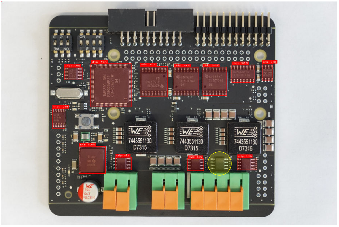
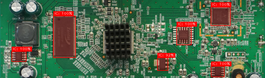
The image above shows detection results of our trained Faster R-CNN model. Correct IC detections are highlighted by red-colored, rectangular areas. Only one IC marked with a yellow circle was not detected by the model. This sample image shows that automated IC detection works pretty well even if both, the IC package and the PCB, have the same color. More information about our approach and evaluation results can be found in the PROBoterthesis and our PROBoterescarpaper .
Pin detection
Besides the location of security-relevant ICs, the positions of the pins connecting these ICs to the underlying PCB are required for an automated electrical probing as a next step. To assist in this task, we chose two different approaches: The first one facilitates the same Neural Networks already used for IC detection. For model training we used our newly created IC-PINS image data set. In contrast to ICs which can be placed on a PCB arbitrarily by designers, IC pins are typically arranged in equally spaced grids at the borders of the IC package. Based on that fact, we also implemented a Classic Computer Vision pipeline for pin detection. The image below shows the intermediate results of each pipeline stage for a sample image of the IC-PINS data set.
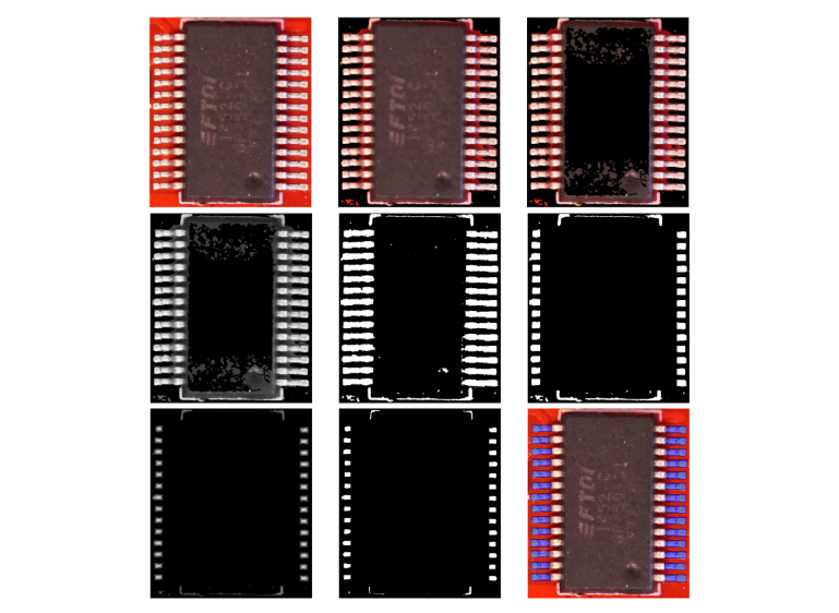
In the first two steps, the border and IC package areas are removed. After that, the individual pins are isolated using color thresholding and morphological operations. Additional skeletonization steps are applied to finally get candidates for IC pin centers. A detailed description of the pipeline can be found in the PROBoterthesis .
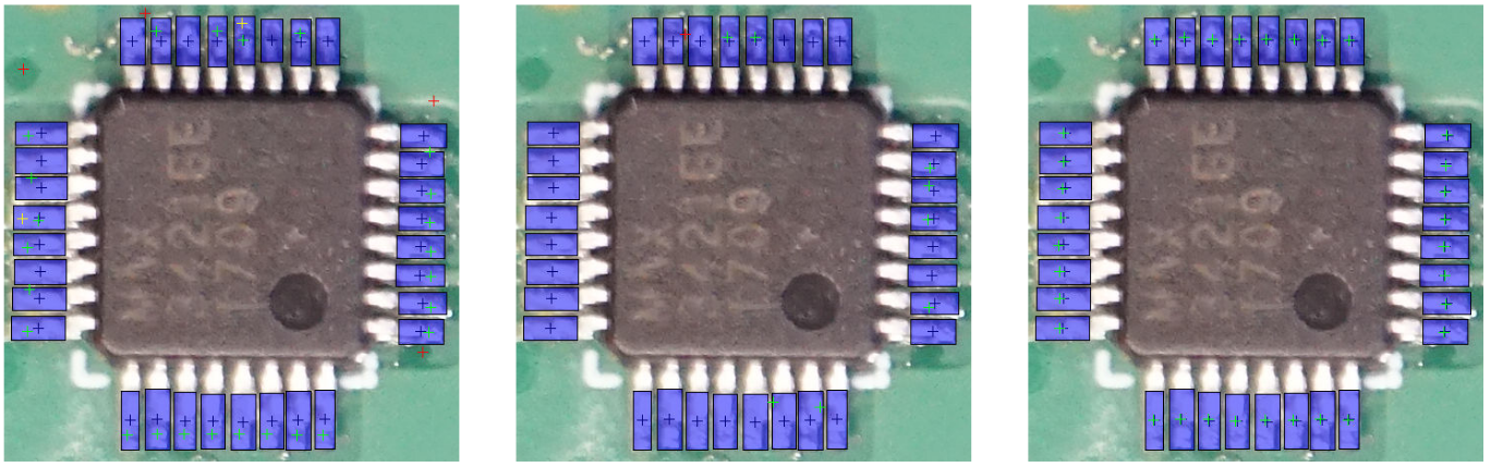
A comparison of the pin detection results is displayed in the image above. The trained Faster R-CNN model yields the best results. However, this approach is the most time and computational intensive. Analysis of a PCB with multiple ICs on a recent CPU-only system can take up to several minutes. Our implemented Computer Vision pipeline is very fast but can produce more False Positive and duplicate detections as can be seen in the left image. Again, you can find more details about the implementation and a thorough discussion of the results in both, the PROBoterthesis and our PROBoterescarpaper . In summary, all implemented solutions still provide options for further approvements. Therefore, we are already working on solutions to further improve automated pin detection.
Show me some code
Up till now, we just explained the theory behind the PROBoter’s approach to automate visual analysis of unknown PCBs. To integrate this functionality in the big picture of the PROBoter framework, we bundled all of the IC and pin detection logic in a single microservice together with our trained Neural Networks. You can find the code of this microservice in the PROBOterGithubrepo . The microservice is written in Python and uses the Flaskframework [5] to expose its functionality via a REST-like web interface. Therefore, integration of this service into your own analysis pipeline is as simple as sending a simple HTTP POST request.
The visual analysis microservice is the first component of the PROBOter software framework. Additional services will be released in the PROBOterGithubrepo with the following blog posts. For an easy setup, all services are additionally bundled as Docker images. As the whole PROBOter framework is constructed of many microservices, we also provide a DockerCompose setup. The Docker Compose file will be extended with the following blog posts and software releases.
Improving image recognition
As mentioned at the beginning, new PCB image data sets have been created in the last few years. The thesis Visualanalysisofprintedcircuitboards [9] created by Marco Günther in cooperation with SCHUTZWERK GmbH examined if the currently implemented algorithms for PCB analysis can benefit from this new image data. The work also extends the Neural Networks in use to detect not only ICs but also connectors and solder pads of unpopulated ICs. These are very interesting probing locations as signals belonging to either debugging interfaces or communication lines are often exposed for development purposes here.
Another major contribution of Marco’s work is the annotation of existing PCB image data sets with labels for different IC packages, like Ball Grid Array (BGA) or QFP (Quad Flat Package). Based on this new information, the Neural Networks have been retrained to not only localize ICs but also to identify their respective package. Because the accessibility of pins depends heavily on the IC package, this adds valuable information that can improve the automated electrical probing capabilities of the PROBoter platform. Integration and evaluation of the results is still ongoing.
We want to thank Marco for his great work and contribution to the PROBoter platform!
Next Post
The next part will introduce novel techniques that can assist an embedded
system penetration tester during the analysis of voltage signals typically
recorded during a black box penetration test. Besides extracting basic signal
characteristics, the developed algorithms can help in the signal line
linking process and protocol identification. Read more in PartIV:Automatedvoltagesignalanalysisandprotocolidentification
.
Follow us on Twitter
, LinkedIn
, Xing
to stay up-to-date.
References / Credits
[1] https://cvl.tuwien.ac.at/research/cvl-databases/pcb-dslr-dataset/
[2] https://github.com/tensorflow/models/tree/master/research/object_detection
[3] https://github.com/tensorflow/models/blob/master/research/object_detection/g3doc/tf2_detection_zoo.md
[4] https://cocodataset.org/
[5] https://flask.palletsprojects.com/en/2.1.x/
[6] PROBoterGitHubrepository
[7] PROBoterpaperDOI:10.13154/294-8348
[8] PROBoterdemovideo
[9] http://dx.doi.org/10.18725/OPARU-40107
This work was sponsored by the BMBF project SecForCARs . We also want to thank igusGmbH for their support and providing hardware samples. The project was created at SCHUTZWERKGmbH (supervisors Dr. Bastian Könings & Msc. Heiko Ehret) in cooperation with HochschuleKempten (examiners Prof. Dr. Elmar Böhler & Prof. Dr. rer. nat Stefan Frenz).