
The PROBoter hardware platform
Part II of the PROBoter blog post series
February 2, 2022
The list below gives an overview of the topics covered in this blog post series. Links will be updated as soon as the corresponding parts are being released.
- PROBoter demo video
- Part I: A platform for automated PCB analysis
- Part II: The PROBoter hardware platform
- Part III: Visual PCB analysis with Neural Networks and classic Computer Vision algorithms
- Part IV: Automated voltage signal analysis and protocol identification
- Part V: The PROBoter software framework
The first part of the PROBoter series gave an introduction to the manual process of embedded system pentesting . It then showed a possible automated workflow which will be implemented in the form of the PROBoter platform. After a longer phase of further internal development and evaluation, this post describes the core component of the PROBoter framework - a hardware platform for automated electrical probing and PCB image generation. The following list summarizes the key features of the PROBoter hardware platform:
- Four autonomous, movable electrical probing units with a positional accuracy in the PCB plane of 0.1 mm
- Working area of the electrical probing units of 300 x 200 x 30 mm (XYZ)
- A static camera system for initial PCB triage
- A movable camera system to generate stitched, high-resolution PCB images with a resolution of 0.1 mm per pixel
- A newly designed signal multiplexer board that allows flexible signal routing, basic measurements like continuity tests and easy adaption of additional measurement and analysis equipment
- An auto-calibration routine that can compensate typical errors resulting from manufacturing or assembling errors
- Open source design. The 3D construction data of the platform can be found in the PROBoter Github repository: https://github.com/schutzwerk/PROBoter/
A Flying Probe Tester for Pentesters
The design of the PROBoter hardware platform is inspired by commercial Flying Probe Testers (FPT). These types of machines are used since the 1980s by PCB manufacturers to ensure the proper functionality of their products at the end of the production line. FPTs are equipped with many, typically up to 8, moving electrical probes which can be freely placed on the PCB under test. The probe movements can be programmed so that the testing routine can be easily adjusted if the board layout changes.
FPTs are highly optimized for accuracy and testing speed. They use high-speed drives to move the electrical probes in combination with high-precision absolute positioning systems to ensure high positional accuracy. To also allow visual board inspection, for example to detect missing or misplaced parts, FPTs are usually equipped with at least one camera system. The price for such machines typically starts at multiple 10k€ and can go up to several 100k€ depending on the ordered machine configuration. Most vendors of FPTs also provide the software to program and control these machines. The software is mostly closed source and extensions can only be provided by or be developed in cooperation with the manufacturer.
In contrast to commercial FPTs, the developed PROBoter hardware platform is completely open source. The construction data and 3D models can be found in the PROBoter Github repository [1]. The mechanical construction was designed from scratch and is based on standard parts that are widely used in state of the art 3D printers. Customized, highly integrated and complex parts are laid out as 3D printable plastic parts. These concepts lead to reduced manufacturing costs and make the replication of the platform affordable for a wide audience. In total, the raw material costs of our assembled prototype of the PROBoter hardware platform added up to around 5000€.
Design
One of the key concept of the PROBoter hardware platform is modularity. The platform can carry up to four probing units which can be added to the platform individually. Therefore, it is possible to start with a minimal setup with only two probes to perform basic tasks like reverse engineering of electrical nets and later add more probes to automate more complex tasks like I2C or SPI bus sniffing with up to four probes.
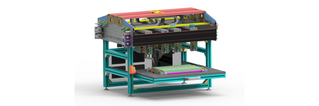
The following image shows a 3D rendering of the current platform design fully equipped with four electrical probing units. As main camera system the current design uses a USB microscope that is attached to one of the four probing units. In addition, a stationary high-resolution camera is mounted at the top of the platform. The individual components will be described in more detail in the following subsections.

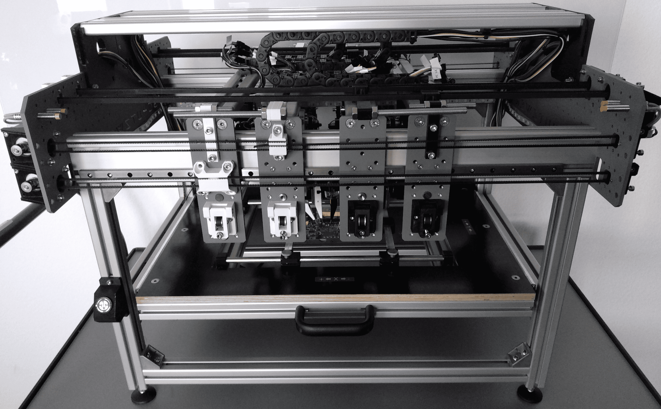
To perform real world tests and evaluations, a prototype of the hardware platform has been built. The image below shows this prototype currently located in our headquarter in Ulm, Germany. If you want to see the prototype in action, check out our PROBoter demo video. The video is part of the SecForCARs project’s demo video series, videos about other parts of the project can be found on the SecForCARs YouTube channel [2].
Base
The base of the PROBoter hardware platform is a frame built of aluminum profiles. It carries a drawer that allows the comfortable placement of the PCB under test outside the machine. At the top, two laser-cut steel plates together with two 60 x 30 mm aluminum profiles form a frame that carries the linear guiding rails for the X axis slides. The X axis uses a profile rail guide which is shared between all probing units. It is driven by stepper motors and a synchronous belt in a Gantry setup. This means that each X axis is moved by two synchronized motors.
Electrical Probing Unit
The PROBoter platform is designed to carry up to four electrical probes. Each probe is carried by a probing unit that is driven by three linear drives. The drives are stacked orthogonally to allow a full 3-dimensional movement of the probe. The image below shows the construction and individual parts of a single probing unit.

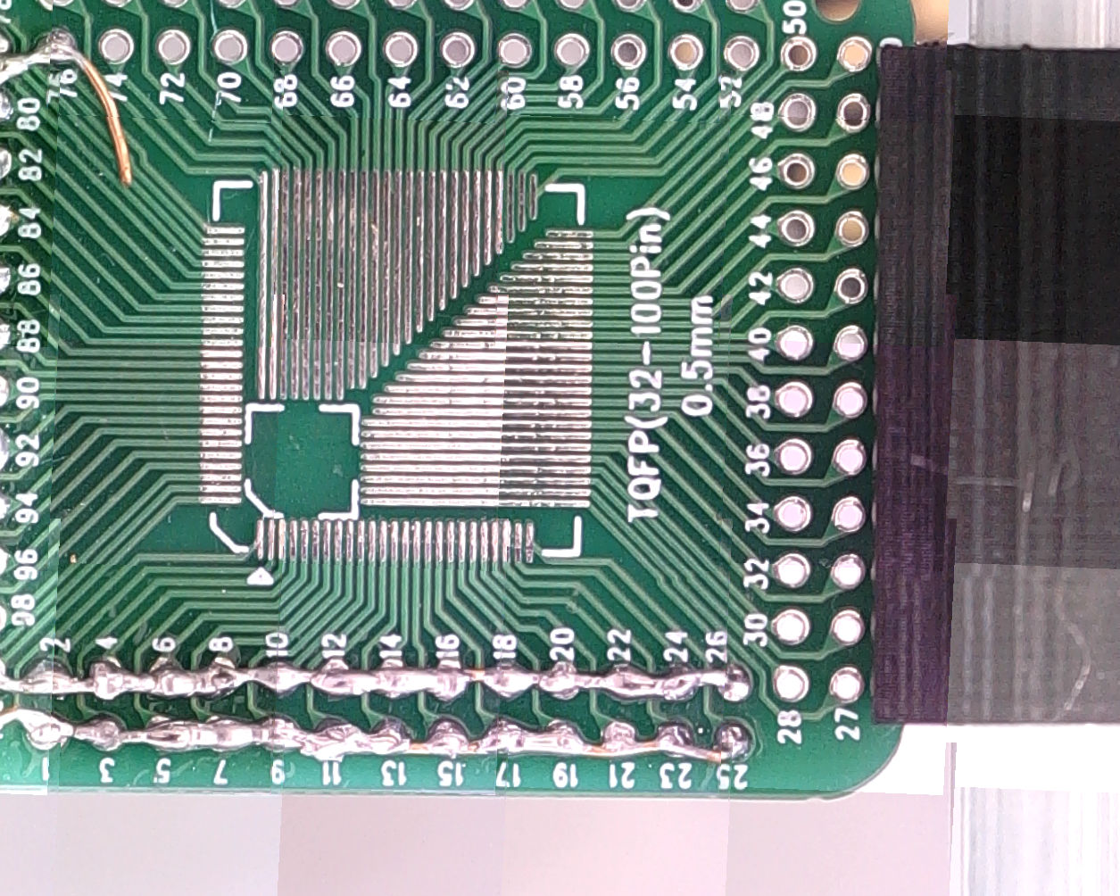
Each unit has a probing volume of 300 x 200 x 30 mm (XYZ) which allows probing of common PCBs. The units are designed so that even if all four probing units are installed, it is possible in theory to position all probes at the same point at the PCB. In the current setup, synchronous belt drives in combination with NEMA 14 and 17 stepper motors are used in all axes. The mechanical transmission of the whole drive system allows an absolute positional accuracy of less than 0.1 mm. This allows probing of TQFP-packaged PCB components with a typical grid size of 0.5 mm and a pad width of 0.17 mm. The X and Y axis can be moved with a speed of max. 100 mm/s or 6 m/min in theory which allows rapid movements and sufficient probing speed.
When started, each axis of a probing unit is homed first. Homing defines the process of moving each axis to a defined position at one of its traveling limits. From there on, the current position in each axis is calculated as the number of moved motor steps multiplied by the mechanical transmission defined by the intermediate drive components. Currently, no further sensors are used to track the axes positions to reduce component costs. An ongoing evaluation phase will show if this open loop control is sufficient to place the probes with the necessary positional accuracy even in long term use.
Camera Systems
Besides the electrical probe, each probing unit can be equipped with a camera system. The camera can then be moved in the XY plane together with the probe. In the current setup, a USB microscope is attached to only one of the inner probing units. This setup allows the generation of high-resolution PCB image data with an absolute pixel resolution of approximately 0.1 mm per pixel which is the same as the accuracy in the probing unit’s drive systems. The high-resolution image generation with the used USB microscope comes with the costs of a limited field of view. To generate a complete image of the PCB under test, the camera system is moved along a predefined path constantly capturing images. From the resulting image data set, the final image can be reconstructed by applying a final image stitching operation. The image below shows the result of this stitching operation for an unpopulated test PCB.
An additional static camera system is mounted at the top of the hardware platform. It can be used for initial triage of the PCB under test. Because the field of view of this camera system covers the whole probing area, the generated images are free of stitching artifacts. However, the absolute mm per pixel resolution is limited. Therefore, for macro views the USB microscope is the preferred image source.
To reduce shadows in the generated PCB images, the platform provides a uniform and diffuse light source through a white LED strip that illuminates the working area.
Signal Multiplexer Board
Even though the electrical probing units can be freely moved in 3D space, there are some movement constraints in the X axis. Because of the shared X guiding system, the probe order is fixed in this direction. Due to this limitation, analysis tools like digital oscilloscopes or other common tools used for embedded system penetration testing like UART to USB adapters or a JTAGulator [3], are not directly connected to the probe signal lines. Instead, these tools are connected to a signal multiplexer board developed at SCHUTZWERK. This board allows flexible routing of signals from the electrical probes to a set of analog or digital outputs. The signal multiplexer can be controlled manually or automated via a text-based control interface exposed over a serial interface.
In addition to signal routing, the board also offers digital to analog conversion functionality. Basic tests like continuity tests can also be performed between two arbitrary signal lines. Therefore, even without additional tools, the PROBoter hardware platform can be used to perform typical time-consuming tasks like electrical net reverse engineering.
Control Logic
The movements of a single electrical probing unit is controlled by a modified version of the open source 3D printer firmware Marlin [4] running on a 3D printer controller board. In our prototype, we used a BigTreeTech SKRv1.3 board [5] for this purpose. Marlin comes with integrated motion control logic and support for dual-motor Gantry setups like the one used for the X axis drives. The firmware is also portable and supports a wide range of microcontrollers and 3D printer controller boards. Movement commands are sent to the controller board as G-codes [6] over a serial interface.
The controller boards are orchestrated by a high-level service implemented in Python. It exposes low-level movement and configuration commands, as well as high-level commands e.g. for PCB image generation via a REST-like web interface. This allows fast and easy integration of the PROBoter hardware platform’s analysis and probing functionality into customized tools or penetration testing workflows. At the moment, a major software refactoring of the PROBoter’s software components is still ongoing. After this process is finished, the source code of the modified Marlin firmware and the Python-based high-level hardware control service will be published on Github.
Calibration
One goal during the design of the PROBoter hardware platform was to facilitate the creation of replica. Therefore, even unskilled or people with little knowledge about mechanical engineering should be able to assemble the platform without special measurement or calibration equipment. Therefore, to compensate most of the errors typically induced during part manufacturing or the later assembly process, the PROBoter platform also features an auto-calibration routine.
For this calibration, a common global Cartesian coordinate system for both, the electrical probing units and the camera systems is introduced. This coordinate system is defined by a 3D printed reference board which is shown in the image below. The corpus of the board consists of a 3D printed part. The yellow-brownish circles represent embedded metallic cylinders made out of brass. The center of each cylinder visible from the top of the board, acts as a reference point in the common coordinate system with well-known absolute coordinates. During the calibration process, these reference points are determined in each unit’s local coordinate system. In the next step, a transformation matrix is calculated that describes the transition from the local to the common global system and vice versa based on the generated point mappings. By concatenating these transformation matrices, coordinates from any unit’s local system can be transformed either in the common global or any other unit’s local system.

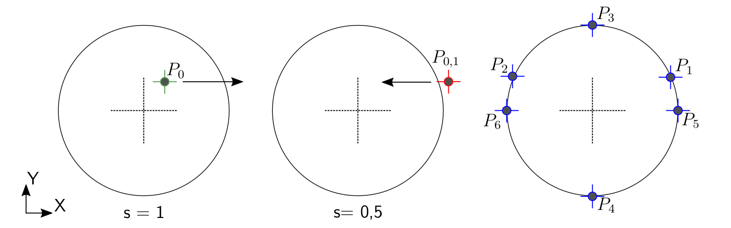
For the electrical probing units, the centers of the metallic cylinders are calculated from four determined points on the cylinder edge. During the calibration process, the probe is connected to a pull-up output and the metallic reference cylinders are connected to ground. A point inside the cylinder is than defined as all locations where the probe’s level is pulled down to ground. Once positioned manually inside one of the reference cylinder’s area, the calibration routine automatically probes six points on the cylinder edge in a cross-like shaped path as can be seen in the illustration below. This scheme is used to maximize the distance between the measurement locations and reduce errors induced by position inaccuracies in the locations of the individual test points. A reference cylinder’s center is finally calculated by performing a circle fit operation using the previously determined edge points. The described steps are repeated for the inner 8 or all 12 reference cylinders.
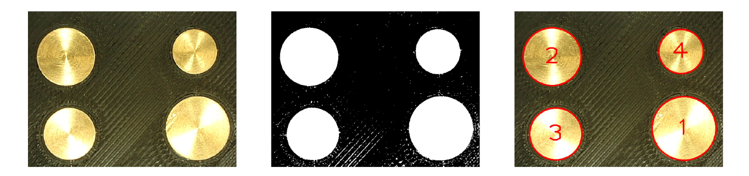
The calibration routines for both, the movable and static camera systems, identify the reference cylinders in a camera image based on the color difference between the reference board corpus and the reference pins. In the image below, the strong contrast in the color of the black reference board and the yellow-brownish brass reference pins is highlighted (left picture). A simple color-based segmentation is used to extract the reference cylinder areas in a camera image (middle picture). The individual reference cylinders are than identified based on their characteristic diameters (right picture). Again, a circle fit operation is used for the final calculation of the reference cylinder centers.
Our evaluation showed that the auto-calibration routine of the PROBoter can compensate most of the mechanical errors. The resulting accuracy in a real world scenario where a user selects a point in an image generated with one of the camera systems and then positioning an electrical probe at this defined location, is in the range of 0.1-0.2 mm. It is therefore sufficient to probe test pads or pins of component packages typically found in an embedded system penetration test. You can find more information about our evaluation methodology and results in our PROBoter paper [7].
Next Post
The next part will show how well-established Neuronal Networks can be
used to automate the initial visual analysis of an unknown PCB. As a result,
possible interesting components like microcontrollers and memory chips are
labeled and the coordinates of the pins that connect these component to the
underlying PCBs are located. So stay tuned :)
Follow us on Twitter
, LinkedIn
, Xing
to stay up-to-date.
References / Credits
[1] PROBoter GitHub repository
[2] SecForCARs YouTube Channel
[3] http://www.grandideastudio.com/jtagulator/
[4] https://github.com/MarlinFirmware/Marlin
[5] https://github.com/bigtreetech/BIGTREETECH-SKR-V1.3/tree/master/BTT%20SKR%20V1.3
[6] https://marlinfw.org/meta/gcode/
This work was sponsored by the BMBF project SecForCARs . We also want to thank igus GmbH for their support and providing hardware samples. The project was created at SCHUTZWERK GmbH (supervisors Dr. Bastian Könings & Msc. Heiko Ehret) in cooperation with Hochschule Kempten (examiners Prof. Dr. Elmar Böhler & Prof. Dr. rer. nat Stefan Frenz).